Founder & Renewable Energy Author, kilowatts.uk


Founder & Renewable Energy Author, kilowatts.uk
Article
Oxford's pseudo-direct semiconductor work is not a UK roof product. The 75% Bi2S3 figure is recombination suppression, not module efficiency.
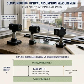
How pseudo-direct semiconductor work, typical output, costs and limits, and whether they have a future for UK homes, balconies and businesses.
A pseudo-direct semiconductor is not a new solar panel you can specify for a UK roof, balcony, factory, or farm. University of Oxford researchers, working with King’s College London, have reported a materials effect in bismuth sulfide, Bi2S3, that keeps strong visible-light absorption while slowing one loss process. The peer-reviewed paper, “Delayed electron-hole recombination in a pseudo-direct semiconductor”, was published in Nature, with the university notice dated 28 October 2026. Oxford PV provided additional support. That is a research link, not a product announcement.
The result does not include a complete solar cell, a module efficiency, a stability test, a manufacturing yield, or a cost. The often-quoted figure of about 75% is suppression of bimolecular recombination at room temperature in the reported experiment, not a 75% rise in panel output. Most carriers were still reported to recombine within roughly 100 nanoseconds because defects remained in control at longer times.
If you are comparing installers or modelling a site, nothing in this work changes irradiance, orientation, shading, temperature, inverter limits, or self-consumption. Certified crystalline-silicon modules remain the equipment that can be designed, connected, and warranted today.
A useful absorber has to do two jobs that often conflict. It must take in sunlight in a thin layer, and it must hold the resulting electrons and holes apart long enough for contacts to collect them. Direct-gap semiconductors tend to absorb visible light strongly. The same electronic structure can also make it easier for an electron and a hole to meet and cancel. That loss is electron-hole recombination.
Bimolecular recombination is the part of that loss that rises as carrier density rises. It is not the only loss. Defects, grain boundaries, and poor contacts remove carriers too. In practice, a laboratory film can look optically promising and still fail as a cell if extraction is slower than those losses.
That is why band-structure engineering matters more here than a single compound name. If absorption and one recombination pathway can be partly separated, device designers gain a rule to hunt for. They do not automatically gain a module.
In this work, a pseudo-direct semiconductor has a direct optical transition, so light is absorbed strongly, plus a slightly lower indirect electronic state. In Bi2S3 that indirect state is reported at about 38 to 40 millielectronvolts below the direct transition. The gap is small in energy terms, which is why carriers can move into the lower state and come back rather than being trapped forever.
The lower state acts as a temporary store, sometimes called a carrier reservoir. Occupation of that store is what the researchers link to slower bimolecular recombination, while the direct transition still provides the absorption. Visible-light absorption was reported above 10^5 per centimetre. That coefficient describes how quickly light is absorbed in the material. It is not a percentage efficiency and it is not a kilowatt-hour yield.
Indirect and direct are statements about momentum in the band structure, not about whether a panel is “almost direct” in a marketing sense. The useful point for non-specialists is narrower. The material can look optically like a strong absorber and still park some excited carriers in a nearby state that recombines less readily by the bimolecular route.
After light creates an electron-hole pair, the carriers have several possible fates. They can be collected as current, recombine with each other, or fall into defects. In the Bi2S3 picture, a fraction of excited carriers occupies the slightly lower indirect state. While they sit there, the bimolecular channel is less active. They can return toward the direct states, which is why the store is described as temporary rather than as a permanent trap.
The reported suppression is about 75% for that bimolecular process at room temperature. Room temperature matters because a UK roof is not a cryogenic lab. A mechanism that only appears when a sample is cooled would be scientifically interesting and commercially irrelevant. This one is claimed at ordinary temperature, which is why it drew attention.
It still does not mean carriers live long enough to be collected in a real device. The same summary says defect-mediated recombination remains, and that most carriers recombine within roughly 100 nanoseconds. Cell design lives or dies on whether contacts and the internal field can extract charge before that happens. Slowing one channel while another still empties the reservoir is a partial win.
The experiment used bismuth sulfide as the material in which the pseudo-direct behaviour could be shown. It was not presented as a finished Bi2S3 photovoltaic product. No flash-test result, datasheet efficiency, temperature coefficient, or encapsulated module is part of the public summary.
The measurements that are described concern electronic structure and carrier dynamics. An indirect state sits only a small energy step below the direct transition. Excited carriers use that state. Bimolecular recombination is reduced by about 75% at room temperature. Strong visible absorption is retained. On longer timescales, defects still dominate.
Those details should be read against the Nature paper, not only against syndicated headlines. Sample form, measurement method, and the exact definition of the 75% figure belong in the paper. Until a reader has that text, it is safer to treat the university notice as the scope of the claim. A carrier-dynamics result can be solid and still be many steps away from a junction, a contact scheme, and an outdoor test.
Panel efficiency is the share of incident sunlight converted to electricity at the module terminals under a stated test. The Oxford figure is a reduction in one recombination rate inside a semiconductor study. Those quantities do not convert into each other. Cutting bimolecular loss by about three quarters could, in a later device, help voltage or current. It could also be swamped by defects, poor contacts, or optical losses in the stack. Nobody has published that device.
Mainstream silicon modules on UK roofs are a different technology, with catalogue efficiencies commonly discussed in the low-20% range for current commercial products. That range is not a result of this experiment and should not be used as a before-and-after comparison. There is no basis here for a payback, a grant, or a generation figure for a pseudo-direct panel, because no such panel has been shown.
The more interesting outcome may be the design rule rather than bismuth sulfide itself. Calculations reported with the paper suggest that particular configurations of tungsten diselenide, WSe2, and indium selenide, InSe, could show similar or greater suppression. Calculation is a screen, not a cell. It does not prove those films can be grown with the required band alignment, low defect density, and stable contacts.
Bi2S3 was a convenient place to demonstrate the reservoir. A commercially suitable semiconductor would still need to be processable as a film or crystal, compatible with electrodes, and stable under heat, moisture, and light. Finding the same electronic pattern in a material the industry can already handle would matter more than optimising the first experimental host.
Oxford PV’s support is worth noting because Britain already has a perovskite manufacturing research base. Support for a study does not place pseudo-direct Bi2S3 in that product line. Perovskite-on-silicon tandems and this carrier-reservoir idea are different technical bets. Conflating them makes procurement conversations less accurate, not more.
Even if the band structure is favourable, defects set the practical lifetime. The summary is explicit that longer-time performance is still limited by defect-mediated recombination. In thin-film photovoltaics that pattern is familiar. A champion flake or single crystal can show clean physics, then a polycrystalline film introduces grain boundaries that act as recombination sites.
It is not known from the available account whether the reservoir survives in a polycrystalline film, at the carrier densities of a working cell, or across the temperature swings of a UK roof. Encapsulation, moisture, and thermal cycling are separate tests. None of them is described here.
Processing questions are also open. Handling, availability, and any toxicity controls for a future process would have to be established by the manufacturers and regulators involved. They are not established by a Nature carrier-dynamics paper. Yield, the share of devices that meet a spec, is unpublished. Without yield, cost talk is speculation.
A genuine photovoltaic step would start with a complete cell. That means a junction, contacts, measured external quantum efficiency, and a power-conversion efficiency under a stated spectrum. A single optical coefficient would no longer be the headline. The next step would be a mini-module that survives light, heat, and damp, not only a fresh sample on a lab bench.
After that, independent module tests, a credible manufacturing route, and a datasheet with temperature coefficients would be the evidence an installer could use. Only then could anyone compare energy yield, degradation, and cost with certified silicon on a British site. Carbon payback and warranty length would also need measured degradation, which does not exist for this result.
Until that chain appears, the honest status is early science. The design rule is the part worth watching. If another semiconductor shows the same reservoir, and a cell then extracts the carriers before defects remove them, the industry case can be reopened. Headlines that skip those steps are not a reason to pause a current project.
Treat this as a research story, not a procurement signal. Homes, small commercial roofs, factories and farms should keep using site-specific yield estimates based on certified modules, shading, and how much electricity is used on site. Delaying an otherwise sound project in hope of a Bi2S3 panel has no published lead time to wait for.
If you follow the science, look for three later signals. A working cell with efficiency and quantum efficiency. Evidence that the reservoir still helps once defects and contacts are in the stack. A named material, which may not be Bi2S3, moving from calculation to a stable device. WSe2 and InSe are candidates in calculations only.
Ask any installer who mentions an “Oxford 75% panel” to show a datasheet and a certification route. If they cannot, they are repeating a misreading. For a system you can build this year, measure your usage, check roof or ground constraints, and compare certified options on warranted performance rather than on laboratory recombination rates. A free home energy survey is the practical next step for a property you can specify now.
Solar comparison
Enter your postcode to assess your roof, compare solar options and connect with trusted UK installers.
Choose home, business or industrial, then enter your postcode. RoboMo maps the roof and ranks panel brands by fit.
1. Postcode Start the assessment for your property.
2. Pin the roof Mark the array on the map.
3. Compare RoboMo™ builds your options.

Battery ROI tool
Enter the day rate, off-peak rate and export rate. The calculator ranks batteries in the Kilowatts shop over 10 years. Home batteries also suit offices and small commercial sites.
Reading

Solar panels want light, not heat. Here's why rising cell temperature cuts voltage and output, and why a cold bright British morning can beat a hot afternoon.
Read article

Roof-integrated solar looks flusher but runs warmer. Here is why the air gap behind an on-roof array matters, and what the trade-off costs in UK output.
Read article
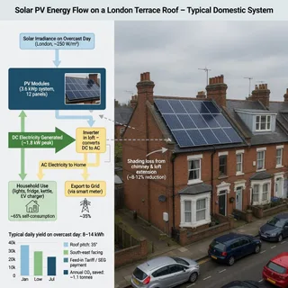
Solar panel installation in London turns on roof area, shade, the lease and UK Power Networks, not the borough. A survey sets the layout and consents.
Read article

Why solar panels make DC, how the inverter converts it to AC at 50 Hz, and why your system shuts down in a power cut unless you have battery backup.
Read article
Write for Kilowatts.uk
Write it here under your own name. Sign in, put a profile up, and start a guide. Pay only if you want more links from your articles out to your own site.
Create a Kilowatts.uk account, or sign in if you already have one.
Put your name, photo and experience on a public author page.
Write a guide or a blog. Free authors can put one followed link to their own site in articles each month.
FAQ
Live help
Talk to RoboMo™ and get instant answers.
Live chat